Rhino Pi A1 Mini Carrier Board Introduction
Product Overview
The Rhino Pi A1 Mini carrier board is equipped with the Rhino Core Q64 smart module. The carrier board features rich data communication interfaces: one 1G RJ45 Ethernet port (with HAT POE power support), an onboard WiFi module supporting WiFi 6 and BT 5.4, USB 3.0 Type-A and USB 2.0 Type-A ports, as well as MIPI DSI, MIPI CSI and HDMI display interfaces. In addition, it supports multiple general-purpose bus interfaces such as SPI, I2C, UART, I2S and GPIO, an onboard PCIe interface for external PCIe devices, and a Micro SD card socket for external storage expansion.
The board is manufactured with strictly selected components and a compact design with rich interfaces, making it easy to integrate into finished products while delivering a smooth experience and strong performance. It can be widely used in industries such as digital signage, touch interaction, consumer electronics and entertainment systems, as well as in robotics, industrial inspection and edge AI scenarios.
Product Appearance
Photo of the Rhino Pi A1 Mini carrier board: 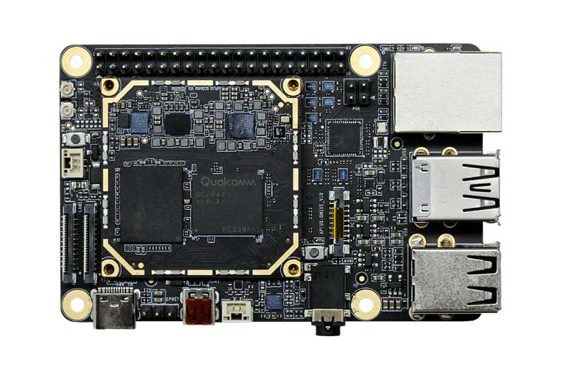
Interface Diagrams
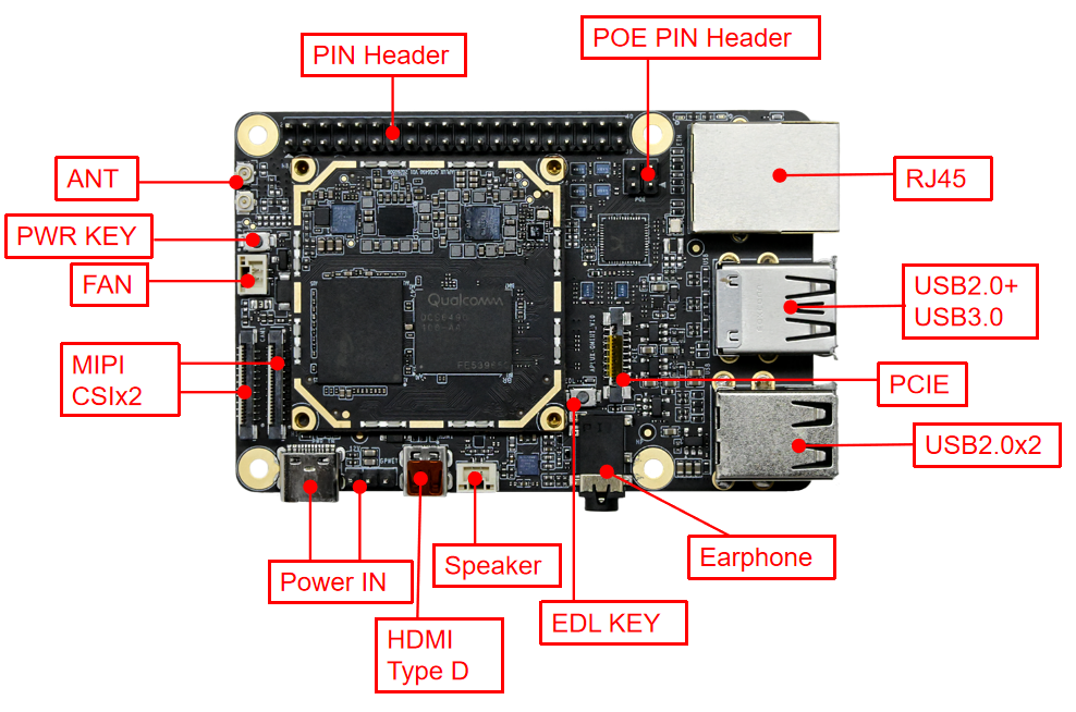
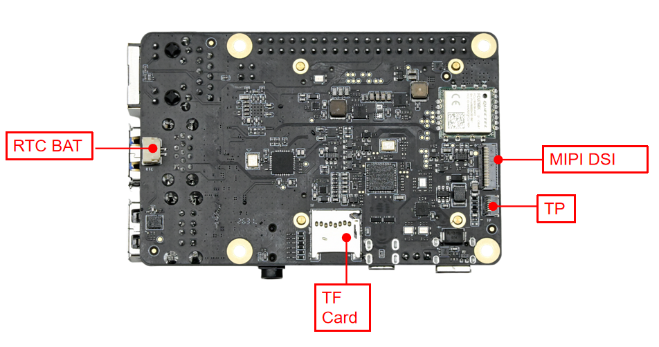
Physical Dimensions
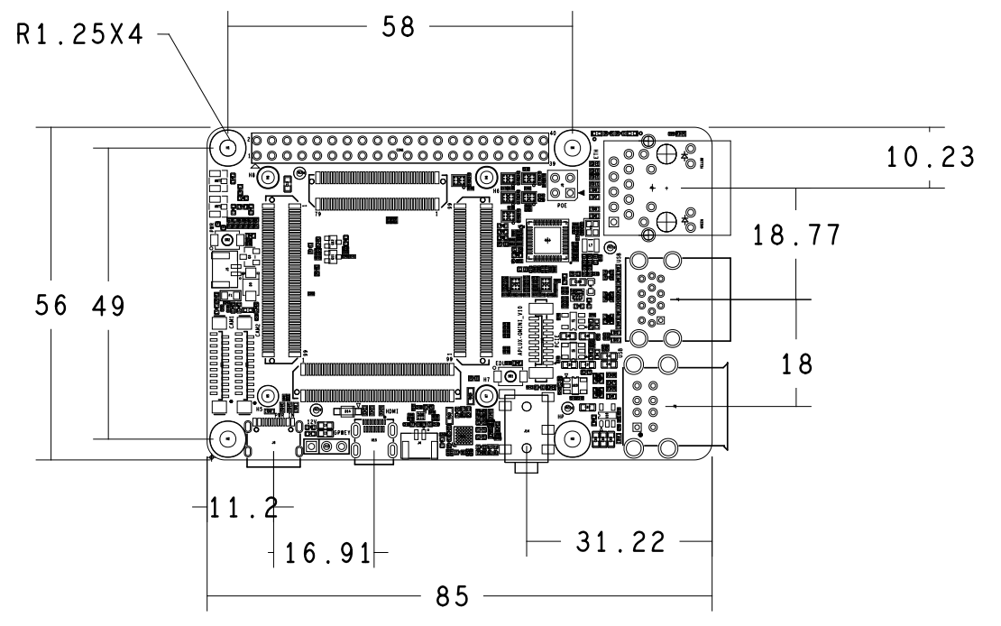
| Item | Parameter |
|---|---|
| PCBA size | 85mm × 56mm (±0.5mm) |
| Board thickness | 1.2mm (±10%) |
| Mounting hole diameter | 5mm |
| Screw hole specification | ∮2.5mm × 4 (±10%) |
For detailed dimension information, contact the APLUX FAE to obtain the DXF document.
Specification List
| Category | Specification |
|---|---|
| Core Board | A6490MA1 core board |
| TF Card | Plug-in TF card socket |
| USB | 4 × Type-A (USB 3.0 ×1 + USB 2.0 ×3) |
| Display | HDMI Type D connector; MIPI DSI display interface |
| Camera | 2 × FPC 22PIN MIPI CSI × 4lane interfaces |
| Ethernet | 1 × 1G Ethernet port with POE |
| Wireless | WiFi 6 & BT 5.4 |
| PCIe | 1 × PCIe FPC 16PIN connector |
| Expansion | 40pin Pitch 2.54mm dual-row header (I2C, I2S, SPI, UART, GPIO) |
| Buttons | Flashing key (RECOVERY) and power key |
| Power Input | 12V/2A, Type-C interface input (PD3.2 adapter supported) |
| Debug | External 3.3V serial debug support |
| Environment | Operating temperature -25°C ~ 50°C, humidity 0%~95% (non-condensing) |
| Dimensions | Length × Width (85mm × 56mm) |
Functions and Interface Definitions
J6 & J12 Power Input Interfaces
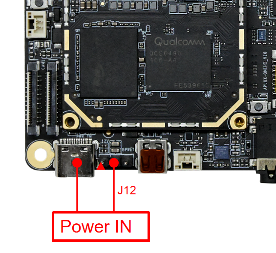
The board supports power supply through either the Type-C interface or the pin header, with a rating of 12V/2A; the Type-C interface is compatible with PD3.2 adapters. The pin header input and the Type-C input must not be used at the same time.
[J6] Type-C power input interface, supporting 12V/2A input and compatible with PD3.2 adapters.
[J12] Pin header power supply, 1×3×2.54mm, where PIN3 is the power-on signal and can be used for an external power button.
PIN Definition:
| Pin# | Definition | Note |
|---|---|---|
| 1 | VCC_12V | 12V input |
| 2 | GND | Digital ground |
| 3 | PWR_KEY | Power-on signal |
J11 RTC Interface
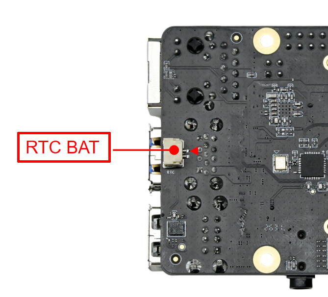
[J11] RTC backup battery interface. An external backup battery is required to use the RTC function. It is a 1×2×1.25mm locking connector, manufacturer: JST, model: SM02B-GHS-TB(LF)(SN).
PIN Definition:
| Pin# | Definition | Note |
|---|---|---|
| 1 | GND | Digital ground |
| 2 | VBAT | RTC battery |
J5 FAN Interface
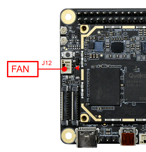
The board provides a 5V fan power interface to support an additional cooling fan, with a maximum current of 1A.
[J5] FAN power socket (1×2×1.25mm), manufacturer: XUNPU, model: WAFER-GH1.25-2PLB.
PIN Definition:
| Pin# | Definition | Note |
|---|---|---|
| 1 | 5V | DC input (5V) |
| 2 | GND | Power ground |
J7 TF Card Socket
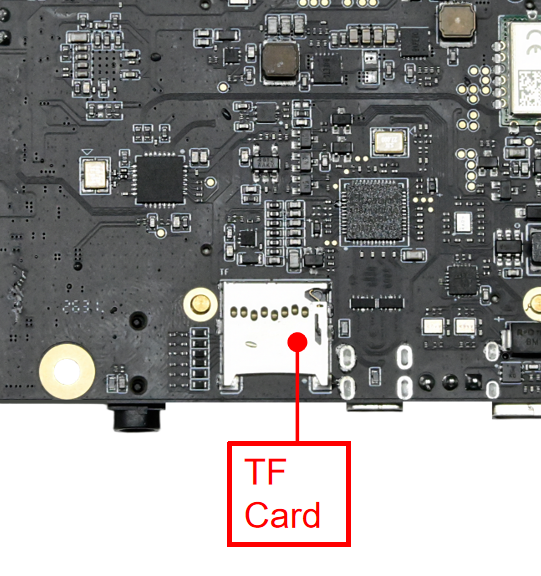
[J7] Plug-in standard TF card socket, supporting SD v3.0 (backward compatible with 2.0).
J1 & J2 USB Interfaces
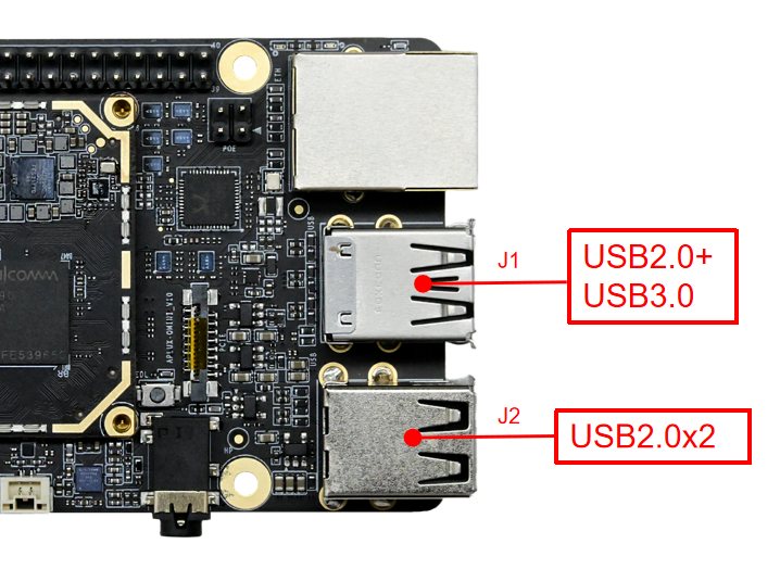
J1 is a dual-deck Type-A USB2.0 + USB3.0 interface, where USB2.0 is expanded from the SoC's native USB2.0 through the GL852 chip, and USB3.0 is the SoC's native USB3.0. Each has its own load switch with a load capacity of 1.2A.
J2 is a dual-deck Type-A USB2.0 interface, both expanded from the SoC's native USB through the GL852 chip; the two ports share one load switch with a total load capacity of 1A.
U15 Micro HDMI Connector
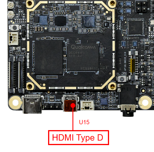
[U15] Micro HDMI connector (HDMI Type D interface).
J55 MIPI DSI Interface
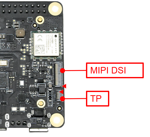
[J55] The DSI interface is 4lane, using a double-sided-contact, flip-type 31PIN FPC connector. Manufacturer: HRS, model: FH35C-31S-0.3SHW(50).
PIN Definition:
| Pin# | Definition | Note |
|---|---|---|
| 1 | LEDA | Backlight anode |
| 2 | LEDA | Backlight anode |
| 3 | LEDA | Backlight anode |
| 4 | - | - |
| 5 | - | - |
| 6 | LEDK | Backlight cathode |
| 7 | LEDK | Backlight cathode |
| 8 | LEDK | Backlight cathode |
| 9 | GND | Digital ground |
| 10 | GND | Digital ground |
| 11 | LN2_P | MIPI DSI data signal |
| 12 | LN2_M | MIPI DSI data signal |
| 13 | GND | Digital ground |
| 14 | LN1_P | MIPI DSI data signal |
| 15 | LN1_M | MIPI DSI data signal |
| 16 | GND | Digital ground |
| 17 | CLK_P | MIPI DSI clock signal |
| 18 | CLK_M | MIPI DSI clock signal |
| 19 | GND | Digital ground |
| 20 | LN0_P | MIPI DSI data signal |
| 21 | LN0_M | MIPI DSI data signal |
| 22 | GND | Digital ground |
| 23 | LN3_P | MIPI DSI data signal |
| 24 | LN3_M | MIPI DSI data signal |
| 25 | GND | Digital ground |
| 26 | - | - |
| 27 | Reset | Display reset signal |
| 28 | - | - |
| 29 | VDD1V8 | LCD 1.8V IO power |
| 30 | 3V3_LCD | LCD 3.3V power |
| 31 | 3V3_LCD | LCD 3.3V power |
[J13] is the TP connector supporting I2C, using a flip-type FPC connector. Manufacturer: HRS, model: FH34SRJ-6S-0.5SH(50).
PIN Definition:
| Pin# | Definition | Note |
|---|---|---|
| 1 | I2C_SCL | I2C clock signal, 3.3V |
| 2 | I2C_SDA | I2C data signal, 3.3V |
| 3 | GND | Digital ground |
| 4 | TP_RST | TP reset signal |
| 5 | TP_INT | TP interrupt signal |
| 6 | VCC_3V3 | 3.3V power output |
J22 & J23 Camera Connectors
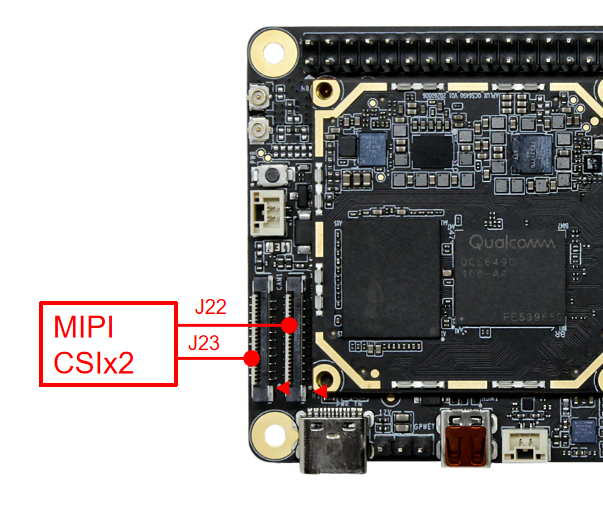
J22 & J23 are camera connectors with identical signal definitions, both supporting MIPI 4Lane CSI with up to 2.5Gbps per lane. They are 1×22×0.5mm vertical drawer-type FPC connectors. Manufacturer: HDGC, model: 0.5K-A-22PB.
PIN Definition:
| Pin# | Definition | Note |
|---|---|---|
| 1 | GND | Digital ground |
| 2 | LN0_M | Differential data signal |
| 3 | LN0_P | Differential data signal |
| 4 | GND | Digital ground |
| 5 | LN1_M | Differential data signal |
| 6 | LN1_P | Differential data signal |
| 7 | GND | Digital ground |
| 8 | CLK_M | Differential clock signal |
| 9 | CLK_P | Differential clock signal |
| 10 | GND | Digital ground |
| 11 | LN2_M | Differential data signal |
| 12 | LN2_P | Differential data signal |
| 13 | GND | Digital ground |
| 14 | LN3_M | Differential data signal |
| 15 | LN3_P | Differential data signal |
| 16 | GND | Digital ground |
| 17 | RST | Reset signal |
| 18 | LED | LED signal |
| 19 | GND | Digital ground |
| 20 | SCL | I2C bus clock signal |
| 21 | SDA | I2C bus data signal |
| 22 | CAM_3V3 | 3.3V power output |
J3 Ethernet Port
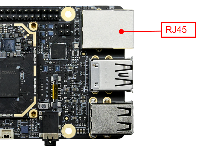
[J3] 1G Ethernet port with POE; the POE function requires a HAT.
J10 PCIe Interface
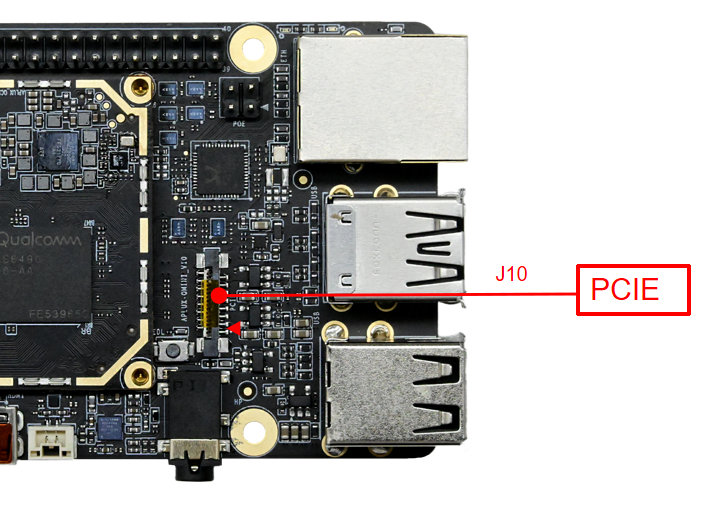
[J10] is a PCIe interface using a vertical drawer-type FPC connector. Manufacturer: XUNPU, model: FPC-0.5AL-16PB.
PIN Definition:
| Pin# | Definition | Note |
|---|---|---|
| 1 | PCIE_5V | 5V output, can power PCIe peripherals, 1.2A |
| 2 | PCIE_5V | - |
| 3 | GND | Digital ground |
| 4 | PCIE_CLK_P | PCIe clock signal |
| 5 | PCIE_CLK_N | - |
| 6 | GND | Digital ground |
| 7 | PCIE_RX_P | PCIe data receive signal |
| 8 | PCIE_RX_N | - |
| 9 | GND | Digital ground |
| 10 | PCIE_TX_P | PCIe data transmit signal |
| 11 | PCIE_TX_N | - |
| 12 | GND | Digital ground |
| 13 | PCIE_PWR_EN | PCIe peripheral power enable signal |
| 14 | PCIE_DET_WAKE | PCIe wake signal |
| 15 | PCIE_CLKREQ_N | PCIe clock request signal |
| 16 | PCIE_RST_B | PCIe reset signal |
CON1 Expansion Interface
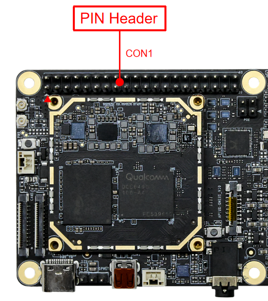
[CON1] External expansion interface, using a 40PIN 2.54mm pitch dual-row header. It can expand I2C, I2S, SPI and UART functions, and can also be used as GPIO. The interface level is 3.3V.
PIN Definition:
| Pin# | Definition | Note |
|---|---|---|
| 1 | VCC_3V3 | 3.3V output |
| 2 | VCC_5V_EXT | 5V output |
| 3 | GPIO44_I2C_SDA_3V3 | GPIO44, default I2C0 |
| 4 | VCC_5V_EXT | 5V output |
| 5 | GPIO45_I2C_SCL_3V3 | GPIO45, default I2C0 |
| 6 | GND | Digital ground |
| 7 | GPIO96_MI2S0_MCLK_3V3 | GPIO96, default I2S |
| 8 | DEBUG_UART_TX_3V3 | Debug serial |
| 9 | GND | Digital ground |
| 10 | DEBUG_UART_RX_3V3 | Debug serial |
| 11 | GPIO25_SPI_MOSI_3V3 | GPIO25, default SPI0 |
| 12 | GPIO97_MI2S0_SCLK_3V3 | GPIO97, default I2S |
| 13 | GPIO16_I2C_SDA_3V3 | GPIO16, default I2C1 |
| 14 | GND | Digital ground |
| 15 | GPIO17_I2C_SCL_3V3 | GPIO17, default I2C1 |
| 16 | GPIO6_UART1_TX_3V3 | GPIO6, default serial ttyHS0 |
| 17 | VCC_3V3 | 3.3V output |
| 18 | GPIO7_UART1_RX_3V3 | GPIO7, default serial ttyHS0 |
| 19 | GPIO49_SPI1_MOSI_3V3 | GPIO49, default SPI1 |
| 20 | GND | Digital ground |
| 21 | GPIO48_SPI1_MISO_3V3 | GPIO48, default SPI1 |
| 22 | GPIO57_FP_SPI_MOSI_3V3 | GPIO57, default SPI2 |
| 23 | GPIO50_SPI1_CLK_3V3 | GPIO50, default SPI1 |
| 24 | GPIO51_SPI1_CS0_N_3V3 | GPIO51, default SPI1 |
| 25 | GND | Digital ground |
| 26 | GPIO55_SPI1_CS1_N_3V3 | GPIO55, default SPI1 |
| 27 | GPIO0_I2C_SDA_3V3 | GPIO0, default I2C2 |
| 28 | GPIO1_I2C_SCL_3V3 | GPIO1, default I2C2 |
| 29 | GPIO27_SPI_CS_3V3 | GPIO27, default SPI0 |
| 30 | GND | Digital ground |
| 31 | GPIO24_SPI_MISO_3V3 | GPIO24, default SPI0 |
| 32 | GPIO26_SPI_SCLK_3V3 | GPIO26, default SPI0 |
| 33 | GPIO56_FP_SPI_MISO_3V3 | GPIO56, default SPI2 |
| 34 | GND | Digital ground |
| 35 | GPIO100_MI2S0_WS_3V3 | GPIO100, default I2S |
| 36 | GPIO59_FP_SPI_CS_3V3 | GPIO59, default SPI2 |
| 37 | GPIO58_FP_SPI_CLK_3V3 | GPIO58, default SPI2 |
| 38 | GPIO98_MI2S0_DATA0_3V3 | GPIO98, default I2S |
| 39 | GND | Digital ground |
| 40 | GPIO99_MI2S0_DATA1_3V3 | GPIO99, default I2S |
Note:
- All the above function pins can be configured as GPIO with a 3.3V level; ensure level matching when connecting external devices.
- The 3.3V and 5V outputs can supply up to 1A.
- The I2C, SPI and UART numbers above are the port numbers in the system.
J14 4-Pole Headset Jack
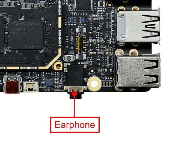
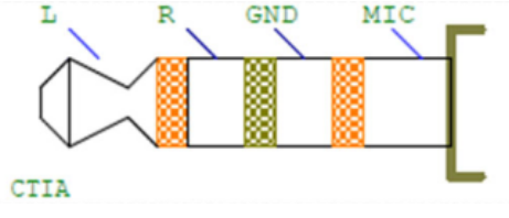
[J14] 4-pole 3.5mm headphone/microphone jack (CTIA standard).
J4 Speaker Interface
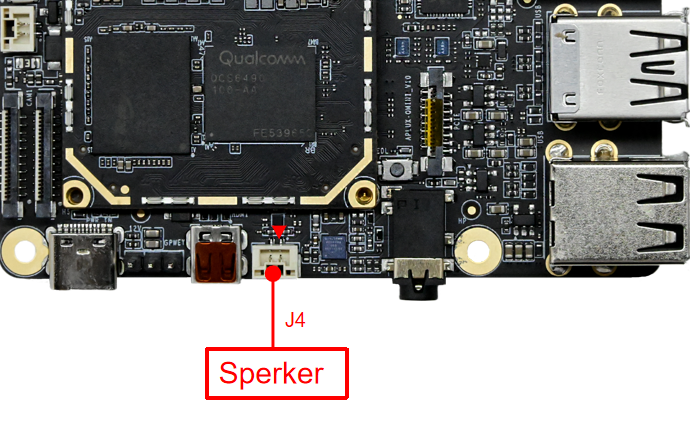
[J4] Speaker interface, 1×2×1.25mm, connector model: WAFER-GH1.25-2PLB, manufacturer: XUNPU. It has an onboard power amplifier with a maximum output of 3.24W×1@4Ω.
PIN Definition:
| Pin# | Definition | Note |
|---|---|---|
| 1 | VO- | Negative BTL audio output |
| 2 | VO+ | Positive BTL audio output |
WiFi/BT Antenna Interfaces
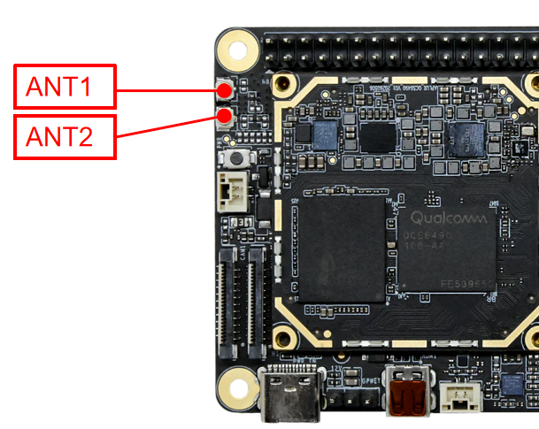
[ANT1 & ANT2] WiFi antenna interfaces (iPEX Gen 1). The board integrates an FCU760K WiFi/BT module supporting WiFi 6 and BT 5.4. ANT1 is the WiFi antenna interface and ANT2 is the BT antenna interface.
SW1 Flashing Mode Button
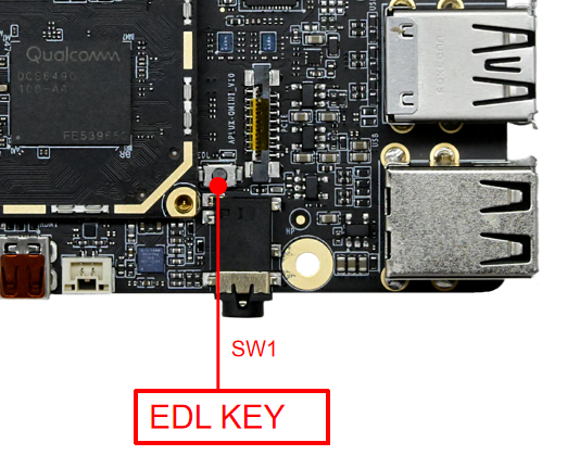
[SW1] SMD flashing button. Press and hold it, then power on for about 3 seconds and release to enter flashing mode.
SW2 Power Button
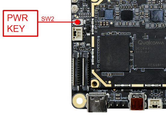
[SW2] Power-on button.
LED
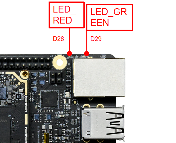
The board has one red LED and one green LED. During normal boot the green LED stays on, and the red LED lights up when the system is abnormal.
Precautions
Please note the following key points when assembling and using the carrier board:
- Relative humidity: 0~95% non-condensing.
- Operating temperature: -25°C ~ 50°C.
- Storage temperature: -45°C ~ 80°C.
- ESD protection is required during assembly and transportation.
- Cables connected to the board's interfaces must not be too long, otherwise signal quality may be affected.
- Do not twist or apply heavy pressure to the board during assembly to avoid deformation.
- Never allow a short circuit between the bare board and other peripherals.
- When connecting external devices to the external interfaces (GPIO, serial, I2C, SPI, etc.), ensure the peripheral I/O levels and currents meet the requirements. When powering peripherals from the power pins on the board's connectors, the current on regular power pins must never exceed 100mA.
Document Information
- Document name: Rhino Pi A1 Mini Carrier Board Product Specification
- Product name: Rhino Pi A1 Mini
- Product code: A6490PZ2-YSQM01
- Version: V1.1
- Release date: 2026-10-13
- Scope: The carrier board and whole-device integration projects based on this hardware platform