Rhino Core Q64 Smart Module Introduction
Product Overview
The Rhino Core Q64 smart module is based on Qualcomm's high-performance, low-power SoC platform QCS6490. The QCS6490 main chip integrates an octa-core Kryo CPU, an Adreno 643 GPU, and a 12 TOPS NPU, designed specifically for industrial control, intelligent inspection, surveillance devices, and edge AI boxes.
This core board features strict material selection and design. Its compact size and rich interfaces make it easy to integrate into complete machines, delivering a smooth experience and powerful performance for end products. It can be applied in industries such as digital signage, touch interactive displays, consumer electronics, and entertainment systems.
Product Appearance
Photos of the Rhino Core Q64 smart module:
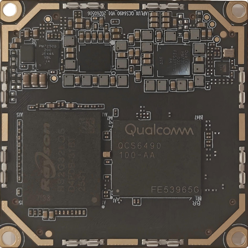
Front
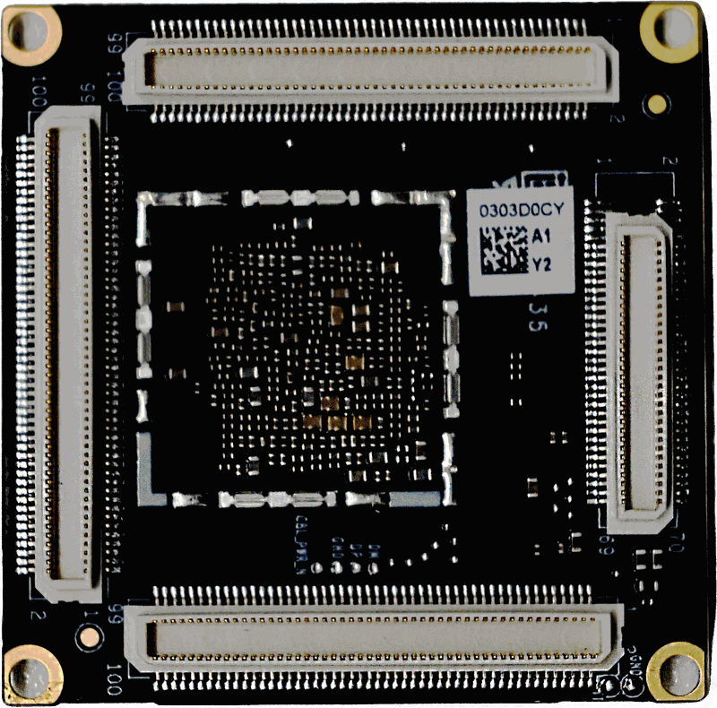
Back
Physical Dimensions
| Item | Parameter |
|---|---|
| PCBA dimensions | 40mm × 40mm (±0.5mm) |
| Board thickness | 1.0mm (±10%) |
| Mounting hole diameter | 4mm |
| Screw hole specification | ∮2.2mm × 4 (±10%) |
For detailed dimensional information, please contact APLUX FAE at noah.yang@aidlux.com.
Product Specifications
CPU
The core board CPU is the Qualcomm QCS6490 in a 1287 PSP package, with chip dimensions of 14.0 × 12.0 × 0.91 mm.
| Item | Parameter |
|---|---|
| AI computing power | 12 TOPS |
| CPU | 1× Kryo Prime @ 2.7GHz + 3× Kryo Gold @ 2.4GHz + 4× Kryo Silver @ 1.9GHz |
| GPU | Adreno 643 |
| Video decoding | 4K@60fps (H.264 / H.265 / VP9) |
| Video encoding | 4K@30fps (H.264 / H.265) |
ROM
The core board supports eMMC 5.1. One 64GB eMMC is populated by default.
RAM
The core board connects to LPDDR5 via the EBI controller, with a maximum frequency of 3200MHz. 8GB LPDDR5 is populated by default, expandable up to 16GB.
Power
The core board uses the Qualcomm PMIC power solution to meet system power supply and CPU power sequencing requirements. It is DC powered with a typical supply voltage of 3.8V.
The core board operating voltage range is 3.5~4.2V, with a maximum current of up to 7A when the CPU and GPU are fully loaded. When powered by battery, ensure sufficient capacitance for VBAT on the carrier board (at least two 47μF capacitors recommended) as well as 5.1V/500mW TVS protection.
Power On/Off
The core board supports two power-on methods: button power on/off and auto power-on. Due to the onboard PM7250B, automatic power-on cannot be triggered via the PM_CBL_PWR_N signal. If power-on via power input is required, a trigger circuit must be designed to satisfy the automatic power-on logic.
Reset and Flashing
The core board exposes the system reset signal and the forced flashing mode signal. Button reset is active-low; the forced download mode should follow the recommended circuit design in the specification.
Peripheral Resource Overview
The core board exposes the following interface resources through board-to-board connectors:
| Connector | Manufacturer | Model | Mating Part Model |
|---|---|---|---|
| J1 / J2 / J3 | Panasonic | AXK600337YG | AXK500137YG |
| J4 | Panasonic | AXK680337YG | AXK580137YG |
| Interface Resource | Qty | Performance Parameter |
|---|---|---|
| CSI | 4 | 4 groups of 4 lanes, supports D/C PHY |
| DSI | 1 | 4-lane MIPI DPHY, supports D/C PHY |
| eDP | 1 | 4-lane eDP interface |
| PCIe | 2 | 1× PCIe Gen3 x2 lanes (supports NVMe) + 1× PCIe Gen3 x1 lane |
| USB | 2 | 1× USB 3.1 Gen1, up to 5Gbps, supports OTG, DP-compatible, supports 4K60 display; 1× USB 2.0 HS |
| SD | 1 | 4-bit, supports SD 3.0 / SDR104, supports dual voltage levels |
| SPI | 4 | 4 groups of general-purpose SPI, master mode only |
| UART | 8 | 1 debug + 1 4-wire UART + 6 2-wire UARTs |
| I2C | 9 | 4 camera-dedicated I2C (CCI) + 2 general-purpose I2C + 3 sensor I2C (SSC) |
| I2S | 2 | 1 non-LPI I2S + 1 LPI I2S (both configurable as PCM or TDM) |
| SWR | 1 | SoundWire, supports PCM / PDM / DATA data formats, supports interrupt wake-up |
| GPIO | 62 | 62 GPIO resources (those marked with * support interrupt wake-up) |
| ADC | 2 | Exposed via PM7325, voltage range 0~1.875V, sampling rate 4.8MHz |
| PWM | 2 | Exposed via PM7350C, can be used for LCD backlight adjustment |
I2C Notes
None of the I2C interfaces have pull-up resistors on the core board. The carrier board design must add pull-ups (2.2kΩ recommended) and it is recommended to reserve 0Ω series resistors on the signal lines. CCI I2C is dedicated to cameras and cannot be used for other devices; SSC I2C is used for sensors such as accelerometers/gyroscopes. The I2C bus level is 1.8V.
SPI Notes
All SPI interfaces reserve only one CS (chip select) signal, support master mode only, and cannot act as slaves. The SPI bus level is 1.8V.
UART Notes
The debug UART is for debugging only and cannot be used for other functions. RS485 / RS232 require a conversion chip designed on the carrier board. For the BT 4-wire UART, it is recommended to refer to our matching mainboard design. The UART level is 1.8V.
VCOIN Power
When VBAT is disconnected and the real-time clock needs to be preserved, the VCOIN power can be used. It is recommended to connect an external large capacitor or coin cell battery; the power consumption after VBAT is disconnected is about 10μA.
Notes
Pay attention to the following key points when assembling and using the Rhino Core Q64 smart module:
- Environmental requirements: Relative humidity 0~95% without condensation, operating temperature -25°C ~ 50°C, storage temperature -40°C ~ 85°C.
- ESD protection: This product is not designed with ESD protection; ESD protection must be designed on the carrier board.
- Level matching: Pay attention to level matching when designing external interfaces.
- High-speed signals: When designing high-speed signal interfaces, follow the design requirements for Layout routing to ensure interface performance. The carrier board design impedance should be consistent with the core board.
Document Information
- Official product name: Rhino Core Q64 Smart Module
- Product alias: Rhino Q64 Smart Module
- Product code: A6490MA1
- Document version: V1.0
- Release date: 2026-07-10
- Classification: Public
- Applicable scope: Rhino Q64 compute module and carrier board/complete machine development projects based on this module
© 2026 APLUX Intelligent Technology Co., Ltd. No part of this document may be copied, distributed, or used beyond the scope defined herein without written permission.