Rhino Boost Q86
Product Overview
Rhino Boost Q86 is a high-performance edge AI compute card from Chengdu APLUX Intelligence Technology Ltd, based on the Qualcomm Snapdragon QCS8625 chipset. It integrates a 60 TOPS (INT8) neural processing unit (NPU) and can stably run large language models (LLMs) and multimodal vision-language models (VLMs) with 0-14B parameters at 13W power consumption, delivering strong local AI compute for edge devices.
The card uses a Mini PCIe form factor and can be quickly integrated into mainstream platforms such as Raspberry Pi and RK development boards through adapter boards. It can also be embedded as a standalone module into various industry terminals.
Product Positioning
Rhino Boost Q86 supports two major application modes:
- Standalone Controller Mode: The compute card runs independently and provides AI services externally via Ethernet (OpenAI-compatible APIs)
- Ethernet Coprocessor Mode: Works with a host board (Raspberry Pi/RK platform). The host handles peripheral management while the compute card focuses on AI inference
Application Scenarios
- Smart Security: Smart NVR, face/abnormal behavior recognition, real-time multi-stream video analysis
- Industrial Field: SOP inspection, component defect detection, robotic arm collaborative control
- Consumer Electronics: Smart NAS, AI live-stream camera, home service robots
- Edge Computing: Edge gateways, local data processing, low-latency interactive terminals
Specifications
| Item | Parameters |
|---|---|
| Platform | Qualcomm Snapdragon QCS8625 (4nm FinFET process) |
| AI Performance | 15 TOPS (FP16) / 60 TOPS (INT8 Dense) / 120 TOPS (INT8 Sparse) |
| CPU | 8-core heterogeneous architecture: 1x3.4GHz + 5x3.2GHz + 2x2.3GHz |
| GPU | Adreno 750, 5.2 TFLOPS-FP16, supports OpenGL ES 3.2 / Vulkan 1.3 / OpenCL 3.0 |
| VPU | Decode: 4K@240fps / 8K@60fps Encode: 4K@120fps / 8K@30fps |
| Memory | 12/16GB LPDDR5X |
| Storage | 128GB UFS 3.1 |
| Network Interface | 2.5G Ethernet (RJ45) |
| Interfaces | Mini PCIe (PCIe Gen3 x2 RC), USB 3.1, USB 2.0, UART, I2C |
| Power Supply | Typical 12V |
| OS | Ubuntu 22.04 |
| Dimensions | 47.0 x 64.0 x 3.25 mm (Mini PCIe package) |
| Operating Temperature | -20C ~ +45C |
Product Appearance
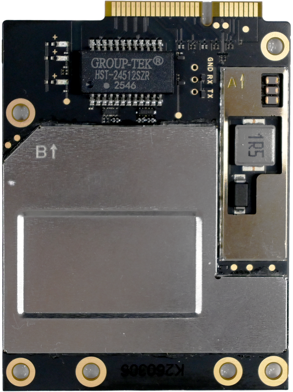
Front
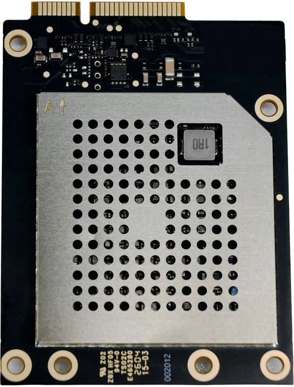
Back
Note
The physical appearance is subject to the delivered product. Images are for reference only.
Mechanical Dimensions
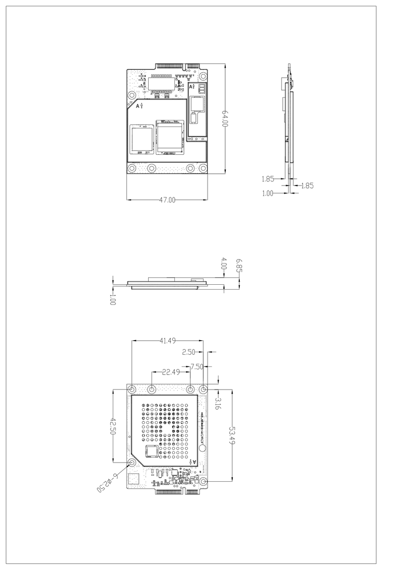
| Item | Parameters |
|---|---|
| Dimensions | 47.0 x 64.0 x 3.25 mm (excluding thermal accessories) |
| Weight | Approx. 15g |
| Operating Temperature | -20C ~ +45C |
| Storage Temperature | -40C ~ +75C |
| Operating Humidity | 10% ~ 90% RH (non-condensing) |
| Cooling Method | Passive cooling (heatsink or active fan recommended) |
Interface Definition
Rhino Boost Q86 exposes all interfaces through the Mini PCIe edge connector, including power, data, control, and debug interfaces.
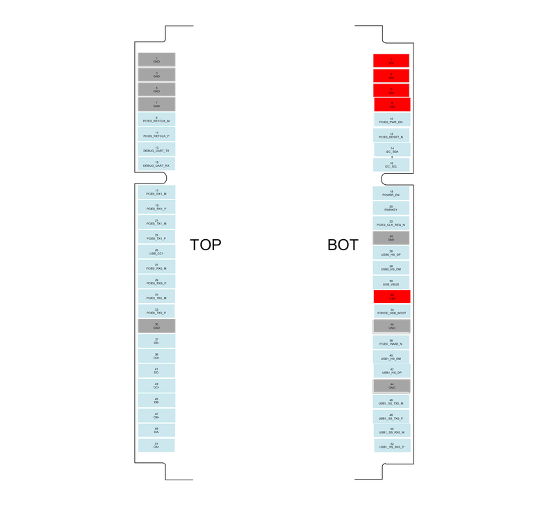
- Interface summary:
| Interface Type | Specification and Function |
|---|---|
| Power Input | 5V~18V wide-voltage input (VCC_IN, Pin 2/4/6/8) |
| Data Interface | 1x2.5Gbps RJ45 Ethernet, 1xPCIe RC Gen3 (2 lane) |
| USB Interface | 1xUSB 3.1 (SuperSpeed), 1xUSB 2.0 (HighSpeed) |
| Control Interface | 1xUART (1.8V, debug serial), 1xI2C (1.8V) |
| Power On/Off | PWRKEY (active low), POWER_EN (power enable) |
| Emergency Download | FORCE_USB_BOOT (pull high to 1.8V to enter EDL mode) |
- Key pin definitions:
| Pin Name | Pin No. | I/O | Description |
|---|---|---|---|
| VCC_IN | 2, 4, 6, 8 | PI | Four input power pins, supports 5~18V wide-voltage supply. Add large capacitors and Zener diodes externally for surge protection. |
| 1.8V-OUT | 32 | PO | 1.8V power output, 100mA. Output is available only after power-on. |
| GND | 1, 3, 5, 7, 35, 24, 36, 44 | - | Ground |
| PCIE0_REFCLK_M | 9 | AO | PCIe reference clock - |
| PCIE0_REFCLK_P | 11 | AO | PCIe reference clock + |
| PCIE0_PWR_EN | 10 | DO | PCIe peripheral power enable, 1.8V level |
| PCIE0_RESET_N | 12 | DO | PCIe reset signal, 1.8V level |
| PCIE0_WAKE_N | 38 | DI | PCIe wake interrupt request signal, 1.8V level |
| PCIE0_CLK_REQ_N | 22 | DI | PCIe clock request signal, 1.8V level |
| PCIE0_RX0_M | 27 | AI | PCIe Lane0 RX - |
| PCIE0_RX0_P | 29 | AI | PCIe Lane0 RX + |
| PCIE0_TX0_M | 31 | AO | PCIe Lane0 TX - |
| PCIE0_TX0_P | 33 | AO | PCIe Lane0 TX + |
| PCIE0_RX1_M | 17 | AI | PCIe Lane1 RX - |
| PCIE0_RX1_P | 19 | AI | PCIe Lane1 RX + |
| PCIE0_TX1_M | 21 | AO | PCIe Lane1 TX - |
| PCIE0_TX1_P | 23 | AO | PCIe Lane1 TX + |
| DD- | 37 | AI/AO | RJ45 differential signal, supports 2.5G and backward compatible with 100M/1000M |
| DD+ | 39 | AI/AO | RJ45 differential signal |
| DC- | 41 | AI/AO | RJ45 differential signal |
| DC+ | 43 | AI/AO | RJ45 differential signal |
| DB- | 45 | AI/AO | RJ45 differential signal |
| DB+ | 47 | AI/AO | RJ45 differential signal |
| DA- | 49 | AI/AO | RJ45 differential signal |
| DA+ | 51 | AI/AO | RJ45 differential signal |
| DEBUG_UART_TX | 13 | DO | DEBUG_TX data output, 1.8V level. Default module debug port. |
| DEBUG_UART_RX | 15 | DI | DEBUG_RX data input, 1.8V level. Default module debug port. |
| I2C_SDA | 14 | OD | I2C signal, 1.8V level. Internally pulled up to 1.8V through 2.2K. |
| I2C_SCL | 16 | OD | I2C signal, 1.8V level. Internally pulled up to 1.8V through 2.2K. |
| USB0_HS_DP | 26 | AI/AO | USB 2.0 differential data positive. When high, module USB2.0 switches to pin 26/28. |
| USB0_HS_DM | 28 | AI/AO | USB 2.0 differential data negative. When high, module USB2.0 switches to pin 26/28. |
| VBUS | 30 | DI | USB power input for USB insertion detection. When high, module USB2.0 switches to pin 26/28. |
| USB1_HS_DM | 40 | AI/AO | USB 2.0 differential data negative. When low, module USB2.0 switches to pin 40/42. |
| USB1_HS_DP | 42 | AI/AO | USB 2.0 differential data positive. When low, module USB2.0 switches to pin 40/42. |
| USB1_SS_TX0_M | 46 | AO | USB 3.1 differential TX - |
| USB1_SS_TX0_P | 48 | AO | USB 3.1 differential TX + |
| USB1_SS_RX0_M | 50 | AI | USB 3.1 differential RX - |
| USB1_SS_RX0_P | 52 | AI | USB 3.1 differential RX + |
Note
For carrier-board package dimensions and pin layout details, refer to the A8625MY1 Hardware Design Guide (contact FAE).
Accessories
Rhino Boost Q86 provides multiple adapter boards and debugging accessories to support access from different host platforms:
| Accessory | Model | Compatible Host | Description |
|---|---|---|---|
| Debug baseboard | A8625MY1-SUB-REVA | Universal | Provides complete debug interfaces, including power, serial, RJ45, and USB |
| Raspberry Pi adapter board | CEK2601-Pi5A8625MY1 | Raspberry Pi 5 | Connected via PCIe FPC cable, jointly developed by Firefly Workshop and APLUX |
Note
For detailed accessory information, see the Raspberry Pi 5 AI Acceleration Solution section.
System Platform
Supported operating systems:
- Ubuntu 22.04 + AidLux Desktop (for graphical development and validation)
Quick Access
 Quick Start
ADB login and basic connectivity verification
 Core Board & BSP
Source retrieval, environment setup, build, and firmware flashing
 Peripheral & Interface Dev
Board introduction, installation, BOM reference, and drivers
 Pi 5 AI Acceleration
Raspberry Pi 5 + Rhino Boost Q86 + CEK2601-Pi5A8625MY1 adapter board
 AI App Development & Deployment
AidLite inference, model optimization, generative AI, and voice
 Resources
System images, tools, and reference design materials
FAQ & TroubleshootingHardware, system, and AI development FAQs and troubleshooting