Rhino Pi A1R Carrier Board Introduction
Product Overview
The Rhino Pi A1R carrier board is equipped with the Rhino Core Q64 smart module and is also compatible with the Rhino Core Q85 smart module. The carrier board features dual Gigabit RJ45 Ethernet ports, USB 3.0 Type-A and extended USB 2.0 connectors, and a variety of display interfaces including MIPI DSI/CSI, HDMI, and eDP. In addition, it supports multiple general-purpose bus interfaces such as SPI, I2C, RS485, UART, I2S, CAN, and GPIO.
It integrates an onboard WiFi 6 + BT 5.3 module (AP6275P), a standard Mini-PCIe interface for 4G communication expansion, a Micro SD card slot for external storage expansion, and audio input/output interfaces.
Product Appearance
Photo of the Rhino Pi A1R carrier board: 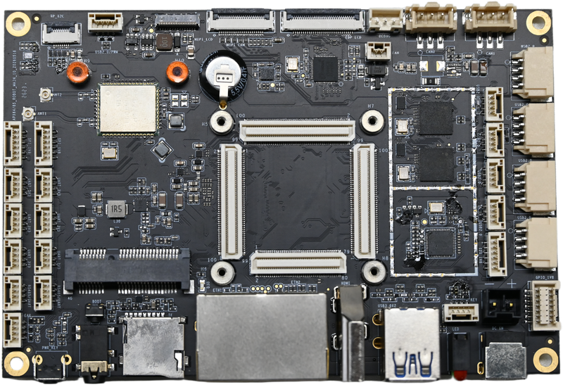
Interface Diagrams
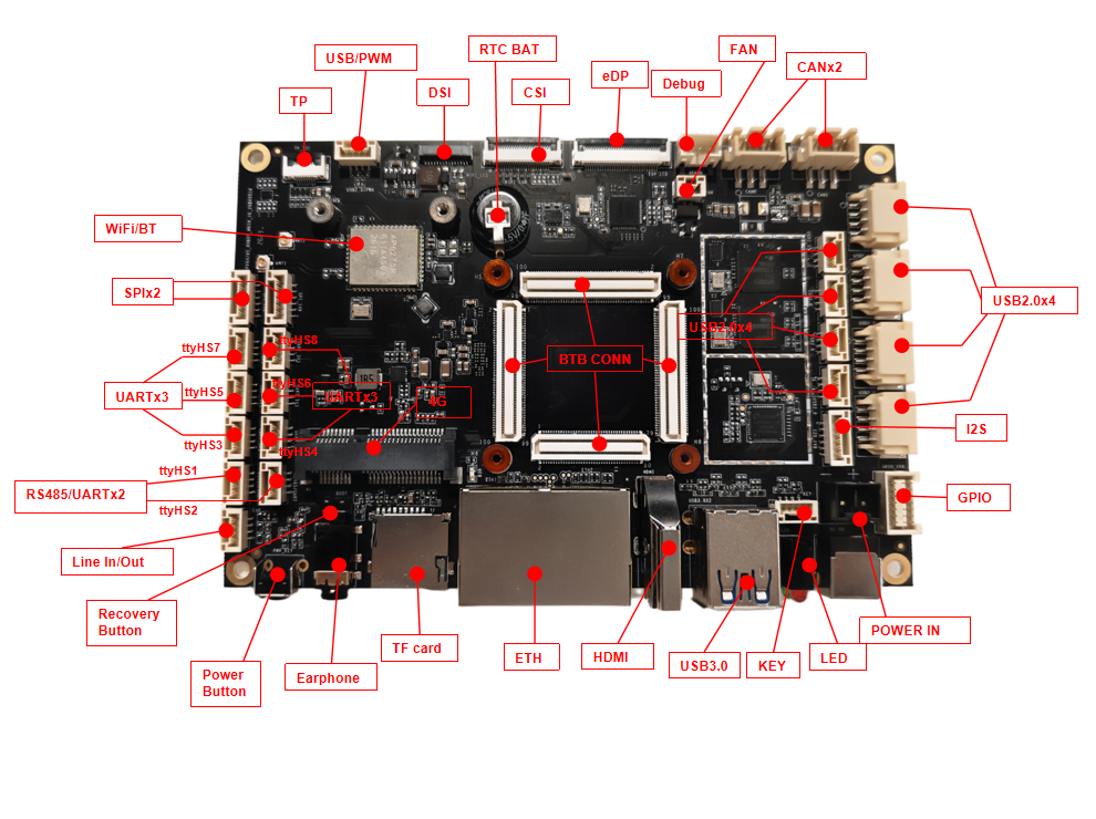
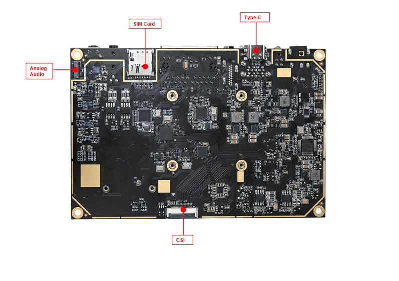
Physical Dimensions
| Item | Parameter |
|---|---|
| PCBA size | 135 mm × 90 mm (±0.5 mm) |
| Board thickness | 1.6 mm (±10%) |
| Mounting hole diameter | 6 mm |
| Screw hole specification | ∮3.2 mm × 4 (±10%) |
| Overall dimensions (including components) | 135 mm × 90 mm × 14 mm, PCB front-side height 9 mm |
For detailed dimension information, contact the Aplux FAE at noah.yang@aidlux.com.
Specification List
| Category | Specification |
|---|---|
| Core Board 1 | Rhino Core Q85 smart module (A8550MA1, optional) |
| Core Board 2 | Rhino Core Q64 smart module (A6490MA1, optional) |
| TF Card | Push-push TF card slot, supports up to 256 GB TF card |
| USB | 2 Type-A ports (USB 3.0 ×2), 4 built-in 1.25 mm latching vertical connectors (USB 2.0 ×4), 4 2.0 mm latching horizontal connectors (USB 2.0 ×4) |
| HDMI | Standard HDMI display interface supporting 4K@60Hz output |
| LCD Interface | Industry-standard 30-pin eDP socket; 4-lane MIPI DSI display interface |
| Touch | FPC interface supporting I2C touch |
| Camera | 2 × 4-lane MIPI CSI |
| I2S Interface | 1 I2S interface |
| Ethernet | 2 auto-negotiation 10/100/1000 Mbps Ethernet RJ45 ports |
| Mini-PCIe | Industry-standard m-PCIe 4G module interface |
| SIM Card | Push-push Nano SIM card slot supporting cellular communication |
| CAN Bus | 2 CAN header interfaces, supporting CAN 2.0B and CAN FD |
| Codec | Low-power voice processing and audiophile-grade playback (supports 4 microphones) |
| Headphone/Microphone | Supports US-standard 4-pole 3.5 mm headset combo jack (L-R-GND-Mic) |
| SPI Bus | 2 individual SPI header interfaces, 1 shared with I2C |
| GPIO | Supports 10 external 1.8V GPIOs |
| Serial Communication | Supports RS485/UART communication, 2 RS485, 6 UART |
| Buttons | Flashing button (RECOVERY) and power button |
| Power Input | Supports 10–24 V wide-range DC input (12 V/3 A recommended) |
| Debug Interface | Supports external 3.3V serial debugging |
| Line Output | Supports standard L/R channel line output (header interface + headphone interface) |
| WiFi / Bluetooth | Onboard WiFi 6 + BT 5.3 |
| Environmental Requirements | Operating temperature -25°C ~ 50°C, storage temperature -40°C ~ 85°C, operating humidity 0%–95% (non-condensing) |
| Physical Dimensions | L × W × H (135 mm × 90 mm × 14 mm), PCB front-side height 9 mm |
| Operating System | Rhino Core Q85 smart module: Ubuntu 22.04; Rhino Core Q64 smart module: Ubuntu 24.04 |
Functions and Interface Definitions
USB 2.0 Interfaces (J8 / J9 / J10 / J11)
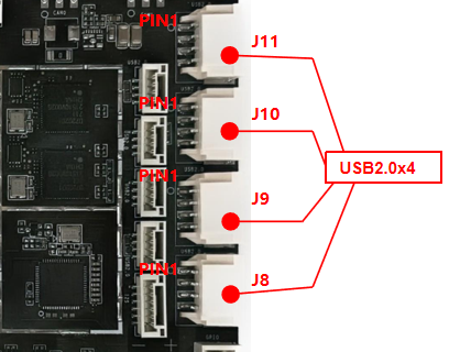
J8, J9, J10, and J11 are all USB 2.0 HOST interfaces, derived from the PCIe-to-USB chip uPD720201K8. Each interface has an independent load switch with a load capacity of 1.2 A. All connectors are 1×4×2.0 mm latching connectors, manufacturer: TXGA, model: FWF20029-S04B25NAM.
PIN Definition:
| Pin# | Definition | Note |
|---|---|---|
| 1 | 5V | 5V output |
| 2 | DM | USB differential data - |
| 3 | DP | USB differential data + |
| 4 | GND | Digital ground |
USB 2.0 Interfaces (J12 / J13 / J14 / J15)
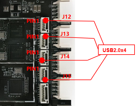
J12, J13, J14, and J15 are all USB 2.0 HOST interfaces, derived via the USB HUB chip FE1.1, so they share a 480 Mbps bandwidth. J12 and J13 share one load switch, and J14 and J15 share another, with a maximum load capacity of 1.2 A per pair. The connectors are 1×4×1.25 mm latching connectors, manufacturer: Xunpu, model: WAFER-GH1.25-4PLB.
PIN Definition:
| Pin# | Definition | Note |
|---|---|---|
| 1 | 5V | 5V output |
| 2 | DM | USB differential data - |
| 3 | DP | USB differential data + |
| 4 | GND | Digital ground |
eDP Connector (J18)
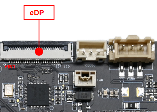
[J18] is a standard eDP connector (1×30×0.5 mm) supporting the eDP v1.4 standard. It is a bottom-contact, front-flip FPC connector, manufacturer: Xunpu, model: FPC-05F-30PH20.
Q64 Adaptation Notes
Since QCS6490 natively supports eDP, the bridge chip on the carrier board is not required if only the 6490 Core Board is used. This motherboard is designed to be compatible with both Core Boards; adapting to different Core Boards requires adjusting the motherboard resistors and capacitors. The eDP backlight must be adjusted according to the input DC power supply: with the default 12 V input, it can be used directly; if 24 V is used, disconnect the direct-connect resistor and populate the power IC (model SY8366HQQC).
PIN Definition:
| Pin# | Definition | Note |
|---|---|---|
| 1 | NC | NC |
| 2 | GND | Digital ground |
| 3 | D1- | Differential data signal |
| 4 | D1+ | Differential data signal |
| 5 | GND | Digital ground |
| 6 | D0- | Differential data signal |
| 7 | D0+ | Differential data signal |
| 8 | GND | Digital ground |
| 9 | AUX+ | Auxiliary differential signal |
| 10 | AUX- | Auxiliary differential signal |
| 11 | GND | Digital ground |
| 12 | LCD_3V3 | LCD_3V3 power output |
| 13 | LCD_3V3 | LCD_3V3 power output |
| 14 | NC | NC |
| 15 | GND | Digital ground |
| 16 | GND | Digital ground |
| 17 | ETX_HPD | Detection signal |
| 18 | GND | Digital ground |
| 19 | GND | Digital ground |
| 20 | GND | Digital ground |
| 21 | GND | Digital ground |
| 22 | BL_EN | Enable signal |
| 23 | BL_PWM | PWM control signal |
| 24 | NC | NC |
| 25 | NC | NC |
| 26 | BL_12V | BL_12V power output |
| 27 | BL_12V | BL_12V power output |
| 28 | BL_12V | BL_12V power output |
| 29 | BL_12V | BL_12V power output |
| 30 | NC | NC |
MIPI DSI Interface (J55)
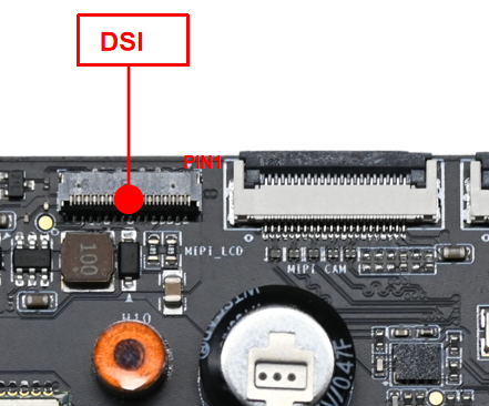
[J55] is a 4-lane DSI interface using a double-sided-contact, flip-type 31-pin FPC connector. Connector manufacturer: HRS, model: FH35C-31S-0.3SHW(50). Compatible panel: Shenzhen Yousee, model: YX80040ACT.
PIN Definition:
| Pin# | Definition | Note |
|---|---|---|
| 1 | LEDA | Backlight anode |
| 2 | LEDA | Backlight anode |
| 3 | LEDA | Backlight anode |
| 4 | - | - |
| 5 | - | - |
| 6 | LEDK | Backlight cathode |
| 7 | LEDK | Backlight cathode |
| 8 | LEDK | Backlight cathode |
| 9 | GND | Digital ground |
| 10 | GND | Digital ground |
| 11 | LN2_P | MIPI DSI data signal |
| 12 | LN2_M | MIPI DSI data signal |
| 13 | GND | Digital ground |
| 14 | LN1_P | MIPI DSI data signal |
| 15 | LN1_M | MIPI DSI data signal |
| 16 | GND | Digital ground |
| 17 | CLK_P | MIPI DSI clock signal |
| 18 | CLK_M | MIPI DSI clock signal |
| 19 | GND | Digital ground |
| 20 | LN0_P | MIPI DSI data signal |
| 21 | LN0_M | MIPI DSI data signal |
| 22 | GND | Digital ground |
| 23 | LN3_P | MIPI DSI data signal |
| 24 | LN3_M | MIPI DSI data signal |
| 25 | GND | Digital ground |
| 26 | - | - |
| 27 | Reset | Display reset signal |
| 28 | - | - |
| 29 | - | - |
| 30 | 3V3_LCD | LCD 3.3V power |
| 31 | 3V3_LCD | LCD 3.3V power |
Camera Connectors (J22 / J23)
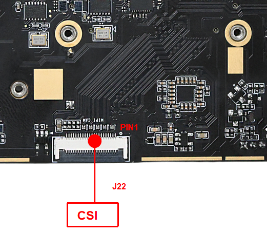
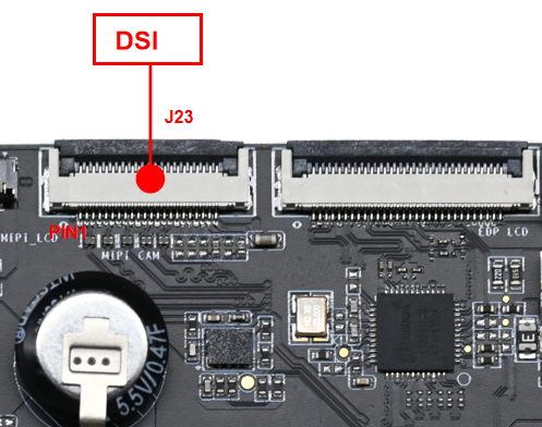 J22 and J23 are camera connectors with identical signal definitions. Both support MIPI 4-Lane CSI with up to 2.5 Gbps per lane. They are 1×22×0.5 mm front-flip FPC connectors, manufacturer: Xunpu, model: FPC-05F-22PH20.
PIN Definition:
| Pin# | Definition | Note |
|---|---|---|
| 1 | GND | Digital ground |
| 2 | LN0_M | Differential data signal |
| 3 | LN0_P | Differential data signal |
| 4 | GND | Digital ground |
| 5 | LN1_M | Differential data signal |
| 6 | LN1_P | Differential data signal |
| 7 | GND | Digital ground |
| 8 | CLK_M | Differential clock signal |
| 9 | CLK_P | Differential clock signal |
| 10 | GND | Digital ground |
| 11 | LN2_M | Differential data signal |
| 12 | LN2_P | Differential data signal |
| 13 | GND | Digital ground |
| 14 | LN3_M | Differential data signal |
| 15 | LN3_P | Differential data signal |
| 16 | GND | Digital ground |
| 17 | RST | Reset signal |
| 18 | LED | LED signal |
| 19 | GND | Digital ground |
| 20 | SCL | I2C bus clock signal |
| 21 | SDA | I2C bus data signal |
| 22 | CAM_3V3 | 3.3V power output |
CAN Connectors (J27 / J28)
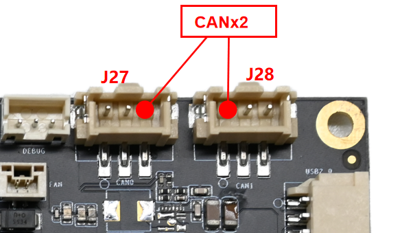 J27 and J28 are CAN connectors with identical signal definitions, supporting both CAN 2.0B and CAN FD. They are 1×3×2.5 mm connectors, manufacturer: TXGA, model: FWF25029-S03S25W5M.
PIN Definition:
| Pin# | Definition | Note |
|---|---|---|
| 1 | H | Data |
| 2 | L | Data |
| 3 | VSS | CAN shield ground |
USB/PWM Interface (J53)
[J53] is a USB/PWM interface (1×4×1.25 mm), connector manufacturer: Xunpu, model: WAFER-GH1.25-4PLB.
Q64 Adaptation Notes
When used with the 6490 Core Board, this interface is USB 2.0 (directly from the Core Board SoC); when used with the 8550 Core Board, it is a PWM output (PM8550 GPIO used as PWM). This document follows the Q64 configuration and treats it as a USB 2.0 interface.
PIN Definition:
| Pin# | Definition | Note |
|---|---|---|
| 1 | 5V | 5V output |
| 2 | DM | USB differential data - |
| 3 | DP | USB differential data + |
| 4 | GND | Digital ground |
RS485 Interfaces (J37 / J38)
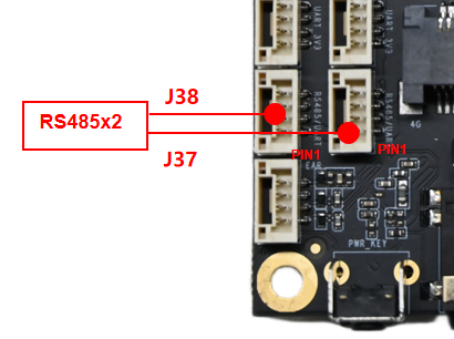 [J37] and [J38] are RS485 interfaces (1×4×1.25 mm) with identical signal definitions, both with onboard 120 Ω termination resistors. Connector manufacturer: Xunpu, model: WAFER-GH1.25-4PLB.
Signal Definition:
| Pin# | Definition | Note |
|---|---|---|
| 1 | VCC | 3.3V power output |
| 2 | B | Differential signal |
| 3 | A | Differential signal |
| 4 | VSS | RS485 shield ground |
UART Interfaces (J39 / J40 / J41 / J43 / J44 / J45)
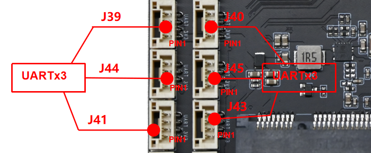 [J39], [J40], [J41], [J43], [J44], and [J45] are UART interfaces (1×4×1.25 mm) with identical signal definitions. Connector manufacturer: Xunpu, model: WAFER-GH1.25-4PLB.
Q64 Adaptation Notes
All of the above interfaces can be used as UART with the 8550 Core Board; with the 6490 Core Board, J44 and J45 can only be used as GPIO (3.3 V level), not as UART.
PIN Definition:
| Pin# | Definition | Level | Note |
|---|---|---|---|
| 1 | VCC | 3.3V | 3.3V power output |
| 2 | TX | 3.3V | Data transmit (TTL) |
| 3 | RX | 3.3V | Data receive (TTL) |
| 4 | GND | 0V | Digital ground |
Precautions
Pay attention to the following key points when assembling and using the Rhino Pi A1R carrier board:
- Environmental requirements: Relative humidity 0–95% non-condensing, operating temperature -25°C ~ 50°C, storage temperature -40°C ~ 85°C.
- Anti-static: ESD protection must be applied during assembly and transportation.
- Cable length: Cables connected to the board's interfaces must not be too long, otherwise signal quality may be affected.
- Mechanical stress: Do not twist or apply heavy pressure to the board during assembly to avoid deformation.
- Short-circuit prevention: Never allow a short circuit between the bare board and other peripherals.
- LCD panel connection: When connecting an external eDP LCD panel, ensure the driving voltage and current meet the requirements, and pay attention to the orientation of pin 1 of the panel cable connector.
- Backlight power supply: When connecting an external eDP LCD panel, ensure the backlight voltage and current meet the requirements. If the panel backlight power exceeds 20 W, it is recommended to use a separate power board for backlight supply.
- Peripheral I/O level and current: When connecting external devices to the external interfaces (USB, GPIO, serial, I2C, SPI, HDMI, etc.), ensure the peripheral I/O levels and currents meet the requirements. When powering peripherals from the power pins on the board's connectors, the current on regular power pins must never exceed 100 mA. Level matching is also required when connecting serial peripherals (1.8 V level, 3.3 V TTL level, and RS-485 level).
Document Information
- Document name: Rhino Pi X1R/A1R Shared Carrier Board Product Specification
- Product name: Rhino Pi A1R Carrier Board
- Product code: A8550PZ1-COM6490
- Version: V1.0
- Release date: 2026-07-20
- Classification: Public
- Scope: Rhino Pi A1R carrier board and whole-device integration projects based on this hardware platform
© 2026 Aplux Intelligent Technology Co., Ltd. No part of this document may be reproduced, distributed, or used for purposes other than those specified herein without written permission.